Part Number: TPS61177A
For LCD Module spec request, may I have your suggest for below pic T1~T4 Timing , I can't find it from spec, thanks !
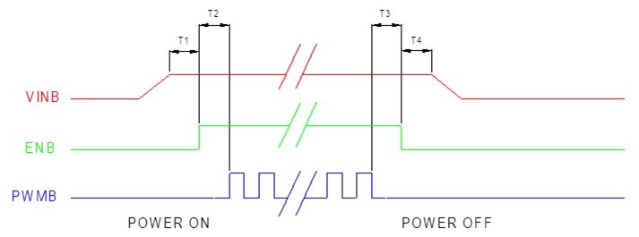
Thanks and Best Regards
James Su
Part Number: TPS61177A
For LCD Module spec request, may I have your suggest for below pic T1~T4 Timing , I can't find it from spec, thanks !
Thanks and Best Regards
James Su
Part Number: TPS65262
Hi Sir,
Can TPS65262 two - way LDO be used in parallel?
What should I pay attention to when using parallel?
Part Number: BQ34Z100-G1
Hi,
Quick question.
Is the QMax Cell 0 parameter for a single cell or the battery pack as a whole? All references to QMax alone refer to the battery pack, but the name of this particular parameter is ambiguous. The bq34z100 -g1 reference document specifies that it should start with the C-rate of the battery (not a single cell), but its name suggests otherwise. Also, the Application Report SLUA664 - Configuring the bq34100 Data Flash states that QMax Cell 0 is "... the maximum chemical capacity of the battery cell".
I have successfully run a learning cycle by using the total battery capacity (4 cells), but wanted to confirm that I was using the correct value to start with.
Regards,
Julian
Part Number: UCC28780
Hello,
I am having an issue with a DCDC converter prototype using the UCC28780. I have chosen the RVS1 resistor for the appropriate brown-in/brown-out voltage desired, yet the actual brown-in threshold observed is much higher.
Additionally, there appears to be no difference between the brown-in and brown-out threshold, whereas the datasheet specifies the brown-out threshold to be 83% of the brown-in threshold.
RVS1: 27K0
RVS2: 8K20
Np: 13
Na: 2
Ns: 4
Vout: 30V
Desired brown-in threshold: approximately 66VDC (with RVS1 = 27K0 I should have 64VDC)
I have set the input voltage to 125V and the converter operates as expected:

CH1 (yellow): QL gate voltage
CH2 (green): QL drain voltage
CH3 (blue): Vbulk
CH4 (pink): Vaux
With a Na/Np ratio of 2/13, a Vbulk of 125V should give approximately 19V for the negative swing of Vaux. The 20.5V measured is pretty close to this.
Measuring the VS pin:

CH1 (yellow): QL gate voltage
CH2 (green): QL drain voltage
CH3 (blue): Vbulk
CH4 (pink): VS voltage
The VS pin is clamping the voltage to -262.5mV, which matches the specified -250mV.
I am not sure if the VS voltage when QL is off should look like this, with the large spike towards the beginning. Perhaps the scope probe is interfering with the signal.
When the input voltage is reduced to below 121VDC, it enters what looks like brown-out detection:

CH1 (yellow): QL gate voltage
CH2 (green): QL drain voltage
CH3 (blue): Vdd
CH4 (pink): Vaux
The switching for 56ms (close to the 60ms brown-out timer) followed by a UVLO cycle leads me to believe this is a genuine brown-out fault.
Zoomed in:

CH1 (yellow): QL gate voltage
CH2 (green): QL drain voltage
CH3 (blue): Vbulk
CH4 (pink): Vaux
When the input voltage is raised above 122VDC, the converter operates as in the first screen capture. There is practically no hysteresis with the brown-in/brown-out.
I feel like I am missing something obvious.
I would appreciate any insight into this problem.
Thanks,
Connor
Dear Engineer,
When I use UCC 28780 design a 65W Active Clamp Converter by referring your reference design such as TIDA-01622A;
I met with some problems. The primary inductance value is 146 uH, Rbur1=196 kOhm, Rbur2=56 kOhm, Nps=6.5; Npa=6.5; Rvs1= 43 kOhm, Rvs2=9.1 kOhm; Rcs =0.17 Ohm;
Rrdm= 95.3 kOhm, Rtz = 300 kOhm, RFB= 22.1 kOhm, Rcomp=540 kOhm, Ccomp =100 pF, Ropp = 1 kOhm. ISO 7710 is used as high-side level-shift.
The start-up process is normal and at 80Vac the circuit could start up normally. But even at the no-load condition, the circuit would enter the AAM mode automatically, with the load current increases, the AAM keeps all the time. Taking the 90Vac input for example, when the load current increases from 0A to 2.4A, the voltage between Rcs is as following. It indicates the negative peak magnetizing current is fixed and the positive peak magnetizing current increases with the load increasing.
I would like to consult how the UCC 28780 could detect the output condition and determine the different operation modes to sustain the stable output voltage such as 20V.
The FB pin, BUR pin, and CS pin all affect the operation mode. But do they affect the operation mode together or individually?
If the circuit enter the AAM mode with complimentary PWML and PWMH signals, what might be the reason to trigger this abnormal operation?
Thanks,
Kailun
Part Number: TPS23758EVM-080
Part Number: LM27762
Background:
We have designed a specialized instrumentation system with embedded micro controller/s.
Basically the instrumentation on board consists of 10 high impedance high voltage monitors and 10 isolated floating current monitors fault tolerant to 1000 VDC, both the current and voltage monitors can both measure an ac and dc component.
The system monitoring system utilizes 2 PGA117, 20 TS12A12511, 20 OPA197, 10 Lmp7715 10 SN6505 and 11 LM27762's.
We designed and had fabricated a PCB to evaluate system function and provide assurance that the system functioned as expected, before changing form factor and commitment to our first true prototype beta. In this first alpha prototype we have implemented only 4 channels of each of the voltage and current measurement sub systems.
Current status:
We have built and tested the supporting circuitry utilizing the on board micro controller and two channels of the current measuring sub system. All seems to be functioning well except the 2 LM27762's in the current measurement system and the lm27762 in the support circuit.
In the support circuit we have designed it for +/- 2.5Volts at 20mA per rail (1). The current measurement circuits lm27762 designed for +/-2.5 Volts at 2-5mA per rail (10).
Most of the systems have been simulated using Tina. The lm27762 have been evaluated using the flash based Web Bench. In addition we tried to directly design using the HTML version of web bench but it reports that the LM72262 is not implemented. We did open the old version design using the HTML version but went back to the old version since it seemed to lack some of the features of the old one. We also exported the design to Tina and have run large number of simulations.
What appears to be happening with the LM72262 is the positive regulator output is as designed, approximately 2.5V and has reasonable regulation with a stepped load. The output is certainly within the tolerance of the internal reference and voltage setting resistors. The problem is with the negative output. Typically it seems to falls into two categories with the three circuits so far implemented. Either no output at all (1-2mV) or a voltage somewhere around -0.8v.
I thought I had put the wrong caps or resistors in place so I removed all components including the LM72262 and placed the caps in first, and measured in circuit are all correct no shorts and connected to the right places. Tested the 4 resistors off board and placed them and checked values in on board including testing for shorts, then placing the LM72262 and checking for shorts and opens using a microscope. Powered up and had exactly the same problems. I went back to Tina and web bench and worked for a day changing the macro models for various esr's and component values including input caps and input supply voltages. Under all of these scenarios I could not reproduce the problem in any simulation.
The board fab house also tested the board to match the layout with no issues. Of course during the simulations the start-up wave forms and running wave forms are different based on values etc but outputs all stabilized to +/- 2.5 Volts. Thinking I may have damaged the device I replaced them with the same result. I decided manually to experiment with different values of capacitor concentrating on the swing cap, cp and the output cap on the negative supply. I discovered by accident, by forgetting to solder cp in place, that I now had the positive supply OK and an incorrect but higher negative output, in some cases -3.6. I put in a lower cp of approximately 1uF and then experimented with the op cap. I found if I reduced this to 1uF as well the negative output started to stabilize at closer to the target -2.5.
I went back to Tina and implemented the changes and the simulation results looked OK
I eventually settled on a 2000pF XR7 cap for the Cp and now I have both the positive and negative somewhat in spec. The positive reg responds OK to a step change in current the negative supply drops a little but is still OK for our needs. On the other two regulators I changed the values to mimic the first regulator, however, I omitted the cp cap altogether and at the lower current requirement they seem to work satisfactorily.
My concern is that the circuits may not be stable in actual use. So finally to get to my question what am I doing wrong to make cp and negative output rail cap so very sensitive. To-date I have also assumed that I may have damaged the devices so I have replaced all of them several times over but all seem to respond in the same way. We have used up at least 10 of my purchase of 20. It should be noted that I am using ESD precautions with the bench and soldering equipment.
Should we persevere with the LM72262 or use different methods to obtain +/- 2.5v at 5-20mA, and if we are to use other devices what would you suggest?
Part Number: BQ25120A
Part Number: BQ40Z60
Hello Team,
Can you help me with a schematic review using the BQ40Z60. I cant attach the schematic but will direct message attach over E2E or email. Thanks for the help!
Part Number: LM73605-Q1
Hi Expert,
I didn't see the detail description about Rsync, could you help to know why need to add Rsync when use external clock ? and why recommend to use 50 to 100 ohm of the terminal resistor?
thanks.
Mark
Part Number: UCC28881
Hi Experts!
I designed a Flyback using UCC28881,
Input power is 300mW,
input DC-rail is regulated at 300V
and we are using a hysteresis control scheme (manipulating the FB pin) to regulate the output voltage at 700V.
However, the efficiency is very low (in the range of 40 ~50%). I know that this IC powers-up from the high-voltage sinking somewhere around 100uA in HVIN pin.
I am trying to limit the peak current to reduce losses and increase the efficiency a bit. Is there any way to do this in this package?
Any other ways to increase the efficiency?
Thanks!
Part Number: BQ76920EVM
The BQ76920EVM is running firmware v1.04. When I start the BQstudio v1.3.93, it says that the auto detected device is 1e9b_1_04 then when I choose 1E9B_1_03_bq78350-R1.bqz from the list, it complains that the detected device is not compatible and the system may enter an unrecoverable state. I also tried with the BQstudio1.3.86.3. The result is the same.
How can I proceed safely ?
Thanks in advance.
Part Number: TPS82085
Hi,
Could you please provide me with the step file for the components listed below (I need the for my power circuitry),
TPS82085
TPS7A8300
TPS82130
TPS7A330
Regards
Samaneh
Part Number: BQ21040
Hi to all, I would like to use BQ21040 to charge LiPo battery.
Previous battery I used had internal NTC resistor (so 3 wires), then batteries are not available, then I had to use simple (2 wires) battery pack.
It's reported BQ21040 uses 10 kOhm NTC: is it safe mount 0805 case NTC resistor on PCB, on direct contact to 18650 battery case?
Also talking about temperature: is it safe keep maximum charge current to 500mA in a sealed enclosure for outdoor portable device or should I go down to 250mA?
Thanks.
Part Number: LP8867-Q1
Hi,
My design goal with LP8867 is to be able to enable or disable individual LED rails on the go, with fault signal properly functioned. I have following design idea and would like some feedback:
- To disable a rail LEDn, disconnect the rail without tying OUTn to GND, and send a 10us reset signal to EN pin to clear the fault.
- To enable a rail LEDn, connect the rail and send 500us reset signal to EN pin.
- My questions is that not tying OUTn to GND is against the datasheet but I'm not sure if it creates a real problem in the long run.
Let me know if there is any concerns with this design or if you have better suggestions.
Thanks,
Borui
Part Number: BQ27750
Hi,
We are trying to program a BQ27750 using bqstudio, EV2400, and .srec, .df.fs, and gm.fs files provided by some colleagues. We placed the device in unsealed mode, flashed the .srec file - no errors, then flashed the df.fs file. There were no errors reported, but bqstudio lost communication with the device. We power cycled and now there seems to be intermittent communication. It sometimes reports reasonable values, such as 20 deg for the temperature reading, but sometimes it reports values like 8192 mA of current, 200059 mV battery voltage (there's no battery connected), -273.5 degC, etc. We do see pulses on the TS line every 500ms, which suggests the firmware is running. We are not able to reprogram it again - we get errors saying "no acknowledge from device." We also periodically see "no acknowledge from device" when trying to refresh the register values.
If the readings from the gauge are to be believed, it seems to be sealed (SEC1 and 0 both 1). When we try to unseal it, a popup appears asking for a key, which is pre-populated with 36720414. We press "ok," but the values of SEC0/1 don't change.
Here are the contents of the df.fs file:
;--------------------------------------------------------
;Verify Existing Firmware Version
;--------------------------------------------------------
W: AA 3E 02 00
C: AA 3E 02 00 17 50 00 04
;--------------------------------------------------------
;Unseal device
;--------------------------------------------------------
W: AA 00 14 04
W: AA 00 72 36
W: AA 00 FF FF
W: AA 00 FF FF
X: 1000
;--------------------------------------------------------
;Go To ROM Mode
;--------------------------------------------------------
W: AA 00 00 0F
X: 1000
;--------------------------------------------------------
;Data Block
;--------------------------------------------------------
W: 16 11 DE 83
X: 200
C: 16 14 FF FF
;--------------------------------------------------------
;Execute Flash Code
;--------------------------------------------------------
W: 16 08 11
X: 4000
Part Number: TPS27S100
Hi,
I have a customer that is looking to use the TPS27S100B and we want to make sure that R_imon is set correctly.
They want to use R_ilm as a backup, so they have it set to 510 ohms which should correlate to ~4.8A.
They want to monitor the current via a 3.3V ADC and turn off the output via the enable pin if the current exceeds 4.5A
Equation [1] in the datasheet shows the R_imon = (V_imon * k_imon) / I_out ... since k_imon is set to 500, setting V_imon to 3.3 V and I_out to 5A (to give some margin) provides a value of 330 ohms for R_imon. Does that seem correct or is there something that I am missing?
Thanks
-Tyler
Part Number: TPS61022
Hello,
I am designing a boost circuit based around the tps61022 chip.
My requirements:
Single cell lipo (3.7v) to boost to 5V 3A (aprox 2.4 amps or so, burst for aprox 2 or less seconds when used with LED)
It is used for a high power LED light with a micro controller .
I used the workbench design tool.

During my testing bench supply as a input at 3.7v. I was able to only get about maybe 1 amp output with the output dropping down to 4.8v (drawing more current would result in the boost chip dying).
I was directed to this help page from the support page.
The components used:
TPS61022
Inductor: SRN8040-1R0Y (digikey part: SRN8040-1R0YCT-ND)
732K resistor: ERJ-2RKF7323X (digi part: P732KLCT-ND)
100K resistor: ERJ-2RKF1003X (digi part: P100KLCT-ND)
Input cap QTY 2: 10uf (CL21A226MOCLRNC, digi part: 1276-6780-1-ND)
Output cap QTY 2: 22uf CL21A226MOCLRNCm digi part: 1276-6780-1-ND
I did try adding a 470uf electrolytic cap, that did not solve my issue.
Speaking to the help person in the original ticket, he suggest to use the parts mention in the datasheet (mainly the inductor).
I have ordered some parts to try and solve the issue:
Inductor as per datasheet: XAL7030-102MEC
10uf ceramic cap, C0805C106K8PACTU
22uf ceramic cap, GRM188R61A226ME15D
47uf ceramic cap, GRM31CR61A476KE15L
As well these are some of my calculation from the datasheet:
| Iout(CL) | Vin | 3.7 | V | |||||
| Equation 5 | IL (DC) | 3.649 | A | Vout | 5 | V | ||
| Equation 2 | Duty cycle (D) | 0.334 | % | Iout | 3 | A | ||
| Equation 6 | IL (P-P) | 1.236 | A | fsw | 1 | MHz | ||
| Equation 7 | IL(P) | 4.267 | n(power conversion efficiency) | 90% | ||||
| Equation 9 | Vripple(ESR) | Inductor inductance | 1 | uH | ||||
Also some scope references:
Measuring inductor at 600 mah load:

Inductor at no load:


Output no load:
Output at 1 amp load

This last screen cap is not great (was from last week not sure if it was accurate/labeled correctly), I can redo it tomorrow when I get the new parts in.
In the mean time:
Did I miss something or miscalculate something?
Any possible idea on why the low output?
Part Number: EV2400
I’m running Windows 10 on a 64-bit system with 8 GB of RAM and a 4.2 GHz processor. I just purchased an EV2400 and BQ27441EVM-G1B. I was able to successfully run 0.28 firmware update, however when I open Battery Management Studio with the BQ27441EVM-G1B connected it automatically comes in the bqStudio Supported Targets window. When I select any of the bq27441.bqz targets I get a message stating “The detected device is not compatible with this application! Some actions could cause the device to lose communication permanently and enter an unrecoverable state. Proceed at your own risk.” When I Cancel out of this bqStudio closes. What am I doing wrong?
Part Number: LM5118
Hello,
I am building a supply that tops off a 940uF capacitor bank at an adjustable ~52.5V
I was able to to get the circuit working but after unplugging/plugging in the 40v input the LM5118 would shut down and stop regulating. The EN pin is tied directly to the Vin.
I am waiting on more LM5118 to do more testing since I burned the first 5.
Any idea what may be wrong based on the circuit?
Best,
-Danny
This the is WEBench circuit that I based my design on:

This the circuit that I have designed and implemented on PCB.
This is the PCB Layout:

