↧
TPS56339: TPS56339 mass production time
↧
TPS3808: please suggest P2P solution to replace XC6118N12AMR-G
↧
↧
TPS767: material content of bond wire change
Part Number:TPS767
We want to know the history that the material content of bond wire was changed from gold wire to copper wire.When the change happened?Was there a PCN document?How many TI part number happened the change?Would you provide the PCN document or the download link?
↧
TPS563201: controlling output ripple of DC DC converter
Part Number:TPS563201
Hi,
In one of my new design, i am using TPS563201 buck regulator to convert 12V DC to 5V DC at output current requirement of 0.5A.
a. Input capacitors placed at Vin are:
1. 10uF/50V ceramic ( 2 Qty)
2. 0.1uF/50V ceramic (1 Qty)
b. Vin and EN pin of buck converter is shorted together.
c. Capacitor (0.1uF/50V) is placed between SW pin and VBST pin
d. inductor value is 3.3uH
e. Output capacitor of 22uF/10V ( 2 Qty)
f. Feedback resistors placed are 56.2K and 10K.
Output ripple coming to be 30mV, but my application required the output ripple to be less than 10mV. I tried to increase the output capacitor but no significant improvement is observed.
Please suggest a suitable way to get the solution.
Thanks
Manish
↧
LM2679: Doesn't reach full output at full load
Part Number:LM2679
Hi Everyone,
I am trying to use the LM2679 to power vacuum tube heaters at 12.2V, 2.7A with an input voltage of 22V. Everything works as expected until I load the circuit to around 1A. Above this, the regulator fails to achieve full output (usually around 7-8V). I've tried quite a few things like raising the current limit from 5 to 7A, changed the soft-start cap from 22uF to 100uF, reduced the output cap and removed the second filter. All have seemed to have helped slightly.
I've made some odd observations that may help one of you with more experience with this chip recognize what is going on:
- The time it takes for the voltage to ramp up seems related to the load current. At 300mA it seems instant, but at 1A it takes 30 seconds of more to get close, at 2.7A we get to around 7-8 max after minutes.
- I will measure no voltage output at either the diode or main cap for a few seconds after startup. The time appears related to load as well.
- This circuit has a standby mode that will reduce the voltage to 8V (actually the circuit starts this way). If I throw the switch for full output before the voltage reaches 8V, it doesn't change the rate of voltage increase...in other words, this doesn't appear to be related to the feedback.
Does anyone recognize this behavior? Anything I should try to get this working? I feel like I'm kind of out of things to do with so few external parts.
Thank you!
↧
↧
TPS23880: TPS23880 Hand Shaking failed
Part Number:TPS23880
Hi Support team
My customer adopted TPS23880 for one port POE power injector, the application circuit is as following, the max power is 45W,they used MSP430FR5969IRGZ for housekeeping MUC and TPS2373-4 EVM-758 for PD to test the function,
the PD would not power up since hand shaking failed, may I have your kindly advice and guide us how to resolve the issue
CH2 is PD output voltage, CH4 is output current,


↧
LM5116: Spike pulse issue of LM5116
Part Number:LM5116
Hi,
I use the LM5116 in our DC/DC design, the input voltage is 9-92V, output voltage is 5V, output current is 0.2A, inductance is 65uH, the switching frequency is 150KHz, we check the voltage of inductance with
your comment for this issue.
.


↧
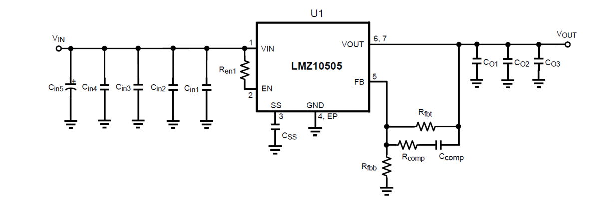
LMZ10505: The value of Rfbb resistance can be 2.2KΩ ?
Part Number:LMZ10505
Dear all
The value of Rfbb resistance can be 2.2KΩ ? I set 2.2KΩ,but when Iout is from1.6A to 3A, the Vout drop to 1.8V from 2.5V, Why ?
↧
TPS2543: Operation Mode for dynamically adjust the current limit
Part Number:TPS2543
My customer is willing to use TPS2543 in a new project, but he has some requirements in the design, so I need your help to find the best way to address this requirements w/ TPS2543. Basically my customer will set TPS2543 to charge at 1.5A or more in CDP mode. During a transient surge that can occur, he needs to reduce the charge current of TPS2543 to zero dynamically and very quickly, while keeping the data lines communicating.
Sounds like the customer will be in the mode S0 --> CTL1/2/3=1 ; ILIM_SEL=1 -->ILIM_HI as per table 2 of datahseet.
So, we think in two possibilities to address this requirement:
1- Based on ds pag 24, sounds like it is needed to go to SDP non charging port (SDP2).
- Is this assumption correct?
- Although it is stated that the port would go to SDP non charging port, in the example, the port goes to SDP w/ 0.9A limit. Would it be the case of changing the I_LIM_LO resistor to any desirable value (e.g. that sets current to <100mA)?
- What would be the timing transition from CDP High Current to SDP2?
2- Using a circuit connected to ILIM_HI ( a resistor in parallel w other w a FET in such way that we can chanve the resistor value dynamically , and that way, the charging current value). Questions:
- Is there any problem of doing this way?
- Will this change be “on the fly”? How long would it take to change the current value once we change the resistor value?
Between those two methods, what would be the recommended to address this requirement? Any other suggestions?
Tks
Raphae Marchi
↧
↧
UCC27712: Spikes on Gate-Emitter during driving of high current in a half bridge with series resonance load
Part Number:UCC27712
Hi ,
We have a Half bridge based Induction heater. The output of the Half bridge is fed into a Series resonance LC (where the L is the Coil of 110uh, and the C is .6uF MKP Capacitor). We have placed around 1.2uS deadtime, which is enough for the IGBT being used.
I m seeing these spikes on the bottom IGBT gate when we are running at a considerable amount of current draw by the half bridge. I have tried lowering the gate drive resistance and increasing the capacitance to reduce these spikes (which I believe are due to dv/dt of the Collector-gate capacitance) .

Here Channel 1 = Low Side IGBT VGC , Channel 2 = High Side IGBT VGC
If this is due to coupling via the Cgc, will a miller clamped isolated IGBT driver help?
Regards,
Tony
↧
CSD87350Q5D: silk of the mosfet is bigger than I bought last time
Part Number:CSD87350Q5D
Dear TI Experts,
I am using TI Mosfet now and the silk of the mosfet is bigger than I bought last time~
I don't know if it's normal?


↧
TPS65580: Multi-layer power inductors for TPS65580 Synchronous Step-Down Converter
Part Number:TPS65580
I would like to use the TPS65580 Synchronous Step-Down Converter in a triple output power supply design. Total output current (around 500ma) is quite a lot lower than the device capabilities. I would like to use smaller and cheaper multi-layer power inductors rather than wire-wound. Can anyone recommend suitable components. I would also be interested in any other recommendations for suitable triple output power converter ICs.
Thanks,
Mark
↧
BQ79606EVM-897: how many EVMs can be stackable ?
Part Number:BQ79606EVM-897
Hi TI expert,
I am confused that the BQ79606-Q1 can be stackable up to 64 devices as described in the datasheet. But why the EVM user guide stated " Up to 51 bq79606EVM
modules can be stacked" ?
Best regards,
↧
↧
LP5562: embedded C driver
↧
BQ34Z651: Heater control not working
Part Number:BQ34Z651
I have the same schematic as the one in the user guide for bq34z651. I am testing the heater control feature in the chip. I have set HEAT ALL and HPOL bits in operation cfg A to 1. Set heater_temp and heater_hys to 20degC. The temperature reading on the chip is 15degC. At this time, the heater should be ON, but is not. I have the OD bit in FET control to be 1. Please let me know if anyone has tested this feature.
↧
LMR23625-Q1: Support Load Dump Test
Part Number:LMR23625-Q1
Hi Expert,
Does LMR23625 could suspport load dump 60V/400mS test? If not, any alternative solution for it? Thanks!
↧
BQ34Z100-G1: reading “Design Energy Scale” from the bq34z100-G1
Part Number:BQ34Z100-G1
I am using a bq34z100-G1 gas gauge and have the I2C interface implemented between an embedded CPU and the gas gauge. I have a question about reading the “Design Energy Scale” that is in the flash subclass 48 and offset 30. Using the technical reference guide, I was able to figure out how to read the flash and I can reliability read the design energy scale value from the flash.
My question is did I miss where I can read this value without having to unseal the device, read it via directly from the flash with the subclass and offset and the re-seal it each time? I was going to write the software on the microprocessor side to read the actual scale factor the gas gauge is using and be able to automatically have microprocessor scale any values from the gas gauge as needed. By having the microprocessor read the actual scale factor and apply it to the readings from the gas gauge, if the golden image ever changes the scale factor, the software on the microprocessor will not need to change.
Did I miss an easier way to read the design energy scale factor without going through the un-seal, read and re-seal? If I really need to unseal the device to read the scale factor and re seal it each time the microprocessor boots, will that hurt the flash memory with by exceeding the flash writes?
Doug
↧
↧
BQ27010: EEPROM Corruption possibly caused by RF introduced on the HDQ signal?
Part Number:BQ27010
Hello, we are having a problem with corrupt registries in the BQ27010 we believed may be caused by spurious RF on the HDQ line introduces from the working environment. Our (1S1P) packs work in a high RF environment and recently we have been having battery packs returned that seem to develop corrupt registry values after a period of time (infant mortality, not defect on arrival). The defective batteries have two symptoms:
1. The battery was fully charged but could not established communications with the host.
2. The battery was fully charged and could establish communications but had corrupt values for a number of registry entries.
For the batteries that don't communicate, forcing a reset by removing interrupting the power resolves the issue and communications ar restored.
For batteries that can still communicate, a reset restore functionality. A cycle test on the restored batteries does not show any registry corruption or anomaly.
The working theory is that the corruptions appear over a period of time until a corruption prevents the battery for communicating at all.
Some registries appear to be more susceptible to corruption.A sample of 38 batteries with this condition showed:
Registry Count Registry Description
Cycles 21 Cycle count invalid, by several orders of magnitude
LMD 15 LMD invalid, by several orders of magnitude
NAC 15 NAC invalid
GPIEN 5 Indicates that a general purpose I/O pin is enabled as an input - incorrect for this battery
PRST 2 Partial Reset – Intended for use during manufacturing.
Other 2 Other registry entries changed
WRTNAC 1 A command to write a new value to NAC - should not be set
This battery has been in use with the same configuration for many years. Previously we had similar results on some prototypes that were missing the zener diode on the HDQ input.
The symptoms are very similar to what is described in SLUA460, ESD and RF mitigation in Handheld Battery Pack Electronics, specifically the sections concerning ESD mitigation "For example, RAM corruption may occur as a result of ESD and is unacceptable if it causes the misreporting of available capacity or other critical information".
We have the typical zener diode protection on the HDQ input and have checked that they are working correctly on the effected packs.
Questions/comments/suggestions? Has there been any changes to the mask/process that might cause this effect? What type of interference on the HDQ input would cause this type of corruption? Any suggestions would be greatly appreciated.
↧
UCC21530: Channel-to-channel isolation voltage, dead-time and overlap protection
Part Number:UCC21530
Hello,
I'm working in a project to develop a new SiC-based 22kW Power Inverter. Currently, I'm looking for a gate driver that will be used for driving two high-side MOSFETs in a three-phase topology.
The UCC21530DWK seems to be the perfect fit for this application considering the UVLO level and the propagation delays.
However, I still have the following questions:
1) Considering the 3.3mm spacing between channels, what is the rated channel-to-channel isolation voltage?
2) I saw in the datasheet that sometimes the gate driver doesn't add the programmed dead-time (Fig. 37, condition C). Why is the gate driver deciding if the dead-time is added or not? What is the benefit?
3) Which is the minimum dead-time that can be programmed using the RDT resistor?
4) We are thinking about using the uC to implement the dead-time. Is there a way to disable the dead-time function of the driver and have only the overlap protection?
Thanks in advance for your help.
↧
UCC21540: DWK package with 3.3mm spacing between channels
Part Number:UCC21540
Hello,
I'm working in a project to develop a new SiC-based 22kW Power Inverter.
Currently, I'm looking for a gate driver that will be used for driving two high-side MOSFETs in a three-phase topology.
The UCC21540 seems to be a good option for this application considering the UVLO level and the propagation delays.
I saw you are offering the DWK option without 2 pins in order to have 3.3mm spacing between the channels.
Maybe this is a trivial question, but why do you use the "K" letter to distinguish between the standard 16 pins package (DW) and the 14 pins?
Thanks.
↧