Quantcast
Channel: Power management forum - Recent Threads
Viewing all 35901 articles
Browse latest View live

BQ27542-G1: How to I find the RB table for my chemistry

$
0
0

Part Number:BQ27542-G1

I'm trying to estimate if the next battery load will drop the voltage below 3.4V before we apply the load. Getting the resistance values from the Ra table was easy but they tend to be a little less than twice my measured values for battery resistance. I saw a note that they are normalized to 0C and I'd like to un-normalize them so I can un-normalize them. 

In : http://www.ti.com/lit/an/slua450/slua450.pdf

R = Ra x exp(Rb x T)

Thanks. 


BQ27542-G1: I set the termination voltage to 3.4V but it still seems to be estimating capacity based on 3.0V.

$
0
0

Part Number:BQ27542-G1

We have a 1.3A is a pulse load with a 3.4V cut off. That is at 3.4V under load I would like the remaining capacity to be 0. The following plot is batter voltage, battery current, and SOC to depict what I mean. 


In the real world case there would be more time between loading and resting but the behavior is similar. 

When I ran a constant discharge it did behave a little better though it was at about half the current so I'll have to run that test again I think. 

TPS56121: Excessive noise due to SW switching.

$
0
0

Part Number:TPS56121

I've a new design using the TPS56121. Vin is 12V and Vout is 1.15V. I am seeing excessive over and under shoot on the rising and falling SW pulse. I've followed the web bench design. And used the recommended devices. I've not put a heavy load on the regulator yet (max 1A).

Is there a minimum load for regulation?

Is there a minimum load requirement?

What is the minimum SW pulse width?

I am using this to drive core voltage on a new ASIC reference design. Please contact me internally via email if possible.

Thanks,

Kevin

TPS650864: Pin Configurations

$
0
0

Part Number:TPS650864

Hi, Team,

We have more questions for the TPS6508640 + ZU6. Could you please support?

1. Could you please let me know how to calculate the below pin components? Is there any documents for this?
33pin; DIFFO
34pin: FB
35pin: COMP

2. Please tell me how to configure the SMBALERT pin when not using.

Best Regards,
Satoshi Yone

TPS24720: SET and SENSE signal routing

$
0
0

Part Number:TPS24720

Hi,

I am using the TPS24720 on my design and i looked at the kelvin routing for the SET and SENSE pins on the TI eval board so that i can try to make it similar on my design. Unfortunately with the location of the sense resistor and the TPS24720, i cannot rout the SET and SENSE signal in the same way. In my layout, SET and SENSE are actually crossed. From the datasheet, it mentions that these signals should be wired side by side but there will be portions of the track that will not be like this due to the cross over. Do i just try and run these side by side for as long as possible and the break into another layer when when i need to run the SET wire to its pin?  Also, how important is it to run the VCC wire next to these wires as per the dev board?

Thanks

TPS82140EVM-720: TPS82130/40/50 EVM radiated EMI scan

UCC21222-Q1: Source & Sink Current(Ioa+/Iob+, Ioa-/Iob-)

$
0
0

Part Number:UCC21222-Q1

Dear, Sir.

My customer is evaluation UCC21222-Q1 for their system.

At this time, They are asking following topics.

Please give your advice.

1. Source & Sink Current(Ioa+/Iob+, Ioa-/Iob-) are defined on the

    datasheet as typical. To calculate the gate charging/discharging time

    min/max would be significant, I think.

    Is it possible to clarify min/max source & sink current?

2. What is the main factor to create above variation?

    Accuracy of the internal current source?

3. I wonder Source & Sink Current(Ioa+/Iob+, Ioa-/Iob-) will keep

    to complete the charging/discharging for Qg of external FET?

4. If Gate & Source was shorted on lowside FET(Source = GND),

    Is there any damage on UCC21222-Q1?

Best Regards,

H. Sakai

TPS5420: leading edge blanking time

$
0
0

Part Number:TPS5420

Hi Team,

D/S mentioned TPS5420 has leading edge blanking time at "Overcurrent Limiting" section. However I can't find actual time spec on this.

Could you share this information?

Regards,

Kotaro Yamashita


TPS2549-Q1: TPS2549-Q1 application question

$
0
0

Part Number:TPS2549-Q1

Hi Sirs,

Sorry to bother you.

In TPS2549-Q1 application, can we set the CS pin with “no connection” condition if we do not need to have power compensation on board?

About the current limitation setting, do you have an EXCEL tool or kind of software that can help engineer to do the calculation?

BQ27542-G1: Chem ID

$
0
0

Part Number:BQ27542-G1

Dear  All:


i have completed chem id cycle and got a report. any one can please double check that the chem id which i get is good for my battery or not.

Battery specification : Tenergy 3.7v 4600mAh Li-ion polymer battery 


Chemistry ID selection tool, rev=2.47

Configuration used in present fit:
ProcessingType=2
NumCellSeries=1
ElapsedTimeColumn=0
VoltageColumn=1
CurrentColumn=2
TemperatureColumn=3

Best chemical ID : 2136 Best chemical ID max. deviation, % : 1.88


Summary of all IDs with max. DOD deviation below 3%

Chem ID max DOD error, % Max R deviation, ratio
2136 1.88 0.16
2019 2.44 0.12
2093 2.46 0.2
2042 2.48 0.1
259 2.53 0.17
2061 2.8 0.1
2056 2.81 0.26
2371 2.83 0.21
2114 2.85 0.11
2099 2.92 0.15

but  I see the  CHEM ID 2136 is  18650D2 3050mAh that  can't meet my battery 6000mAh.  why cause the result?  there is  a   protector of the battery attached,Is that a problem? Thanks~

BQ76930: BQ76930 VC5X damage

TPS54531: unstable at heavy load for 8.1V to 7V buck circuit

$
0
0

Part Number:TPS54531

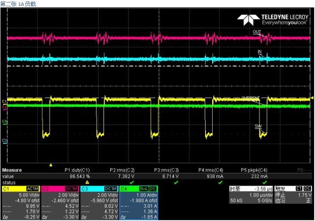
Hi, my customer designed a circuit for input: 8-24V , output: 7V with TPS54531.

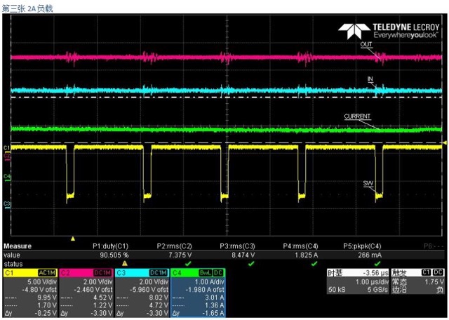
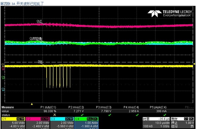
They tested with 8.1V input, the waveform is as below:

with 1A load it's behaving well, red- output voltage, yellow- PH node

with 2A load it's also good, red- output voltage, yellow- PH node

with 3A, the PH node waveform starts to oscillate.

with 3.5A load, the waveform is more distorted and the device will stop working for a while and restart working.

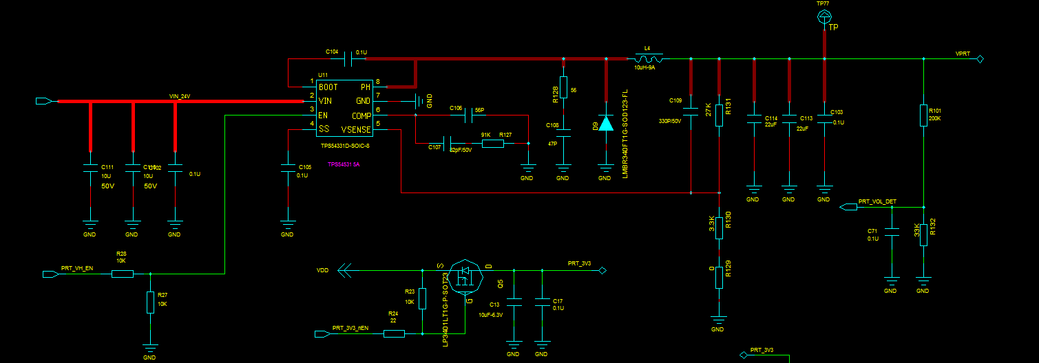
The schematic is as below:

Are there any inappropriation? Especially the RC value at COMP pin.

BQ34Z100-G1: After learning, the capacity exceeded expectations

$
0
0

Part Number:BQ34Z100-G1

as the picture shows:
     According to the self-learning process of the manual, the status is updated to 06, and the RA is updated to 0055, indicating that the learning is successful. After successful, the full charge capacity is 17550, and the actual capacity is 16ah, which exceeds too much, resulting in an error in the estimated battery percentage. , 58v should reach 100%, but now it is 92, how can I solve this problem?


配置文件:

(Please visit the site to view this file)

BQ24032A: Apply high logic level at ISET2, CE and PSEL with dual inputs

$
0
0

Part Number:BQ24032A

Hi

The ISET2, CE and PSEL pins must correct configured during power on. My design has two input: USB and AC (with a 7V solar panel). 

My question:

I need to apply a high logic level (vcc) CE and PSEL. How can I get the correct logic level? Note that USB and AC have diferente voltages and either one can be missing.

BR

Gilberto


LM73605: L/S MOS current limit spec

$
0
0

Part Number:LM73605

Hi,

LM73605 is 5A buck converter, may I know why its minimum threshold of low-side current limit is 4.79A that is less than 5A?

Best regard,

Tiger


BQ25890H: BQ25890H QC2.0 Question.

$
0
0

Part Number:BQ25890H

Dear TI Team,

I am wondering if it is possible to operate according to the specification of QC2.0 when configuring with the following block.

Can the Charger side tell me how to adjust the voltage?

Can you check if the voltage is automatically changed by the current of CC line or D + / D- line through the algorithm of MCU?

And if you use S / W provided by TI, I wonder if it is not a license problem for Quick Charging unless you use QC2.0 phrase.

Thanks.

TPS3420: push button solution which will keep status

$
0
0

Part Number:TPS3420

Hi expert,

Customer is asking for solution which is similar like TPS3420 but will need to keep low or high status for output and toggle status to high or low at next pulse generated by push button. Do we have solution could support this application? Thanks a lot!!

Best regards,

Ann Lien

TPS65720: PB_IN Input

$
0
0

Part Number:TPS65720

Hi TI,

PB_IN Input pin is pulled high in a reference schematic and datasheet.

This pin can be connected with pull-down resistor? So I will connect with MCU('H' signal) when I need.

BQ25713: BATDRV operation in supplement mode

$
0
0

Part Number:BQ25713

According to datasheet, BAT FET works as ideal-diode in supplement mode.

How doest BATDRV output operate?

Does BATFET become fully on when VSYS voltage decrease below VBAT - VF(parasitic diode of FET)?

In my test with EVM, BATDRV voltage became about 6V when VSYS voltage drops to about 7.9V from 8.4V by VINDPM.

Why did BATDRV become about 6V? Is it 0V (VSYS - 10V) if it is full on state?

Best Regards,
Kohei Sasaki

LM25118-Q1: Incorrect output

$
0
0

Part Number:LM25118-Q1

Hi,

Customer of mine is evaluating LM25118-Q1 with their own board. The specification is as below:

Vin = 12V
Vout = 15V
Iout = 3A

However, the measured Vout is only ~9.3V
I've checked the feedback resistor, it seems to be correct.

I attach the schematic, could you help to check what is wrong with the components value or connection?

Thanks!

Viewing all 35901 articles
Browse latest View live


<script src="https://jsc.adskeeper.com/r/s/rssing.com.1596347.js" async> </script>